The wide range of applications of nanofabrication and characterization extends from the communications and entertainment systems in homes to uses in biology, quantum computation, energy generation, medicine and environmental sensing.

Overview

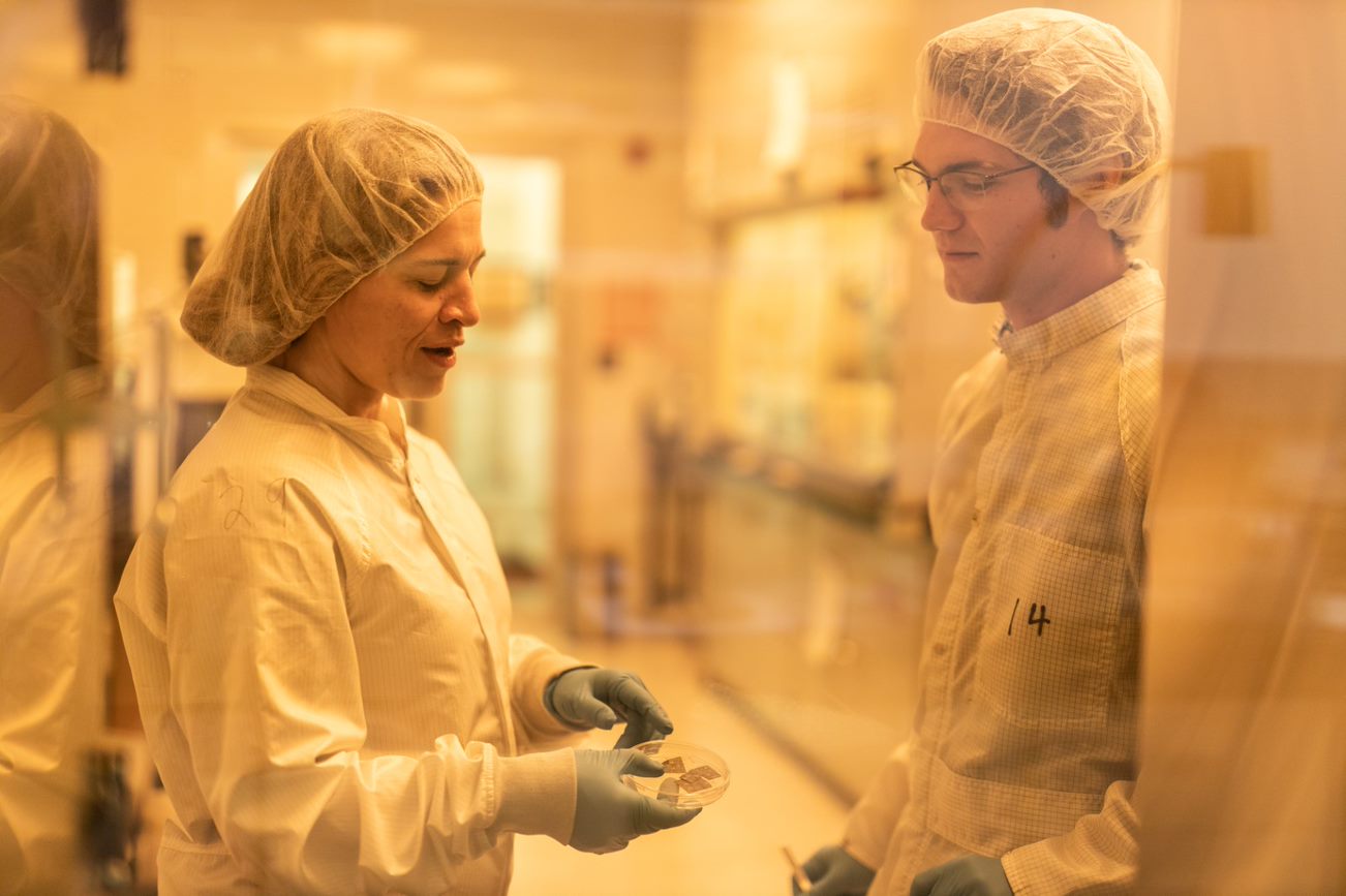
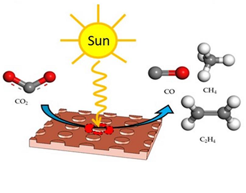
At the University of Ottawa, our world-class researchers are working on several ongoing projects. The results of the activities of the NanoFab will assist with:

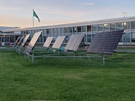
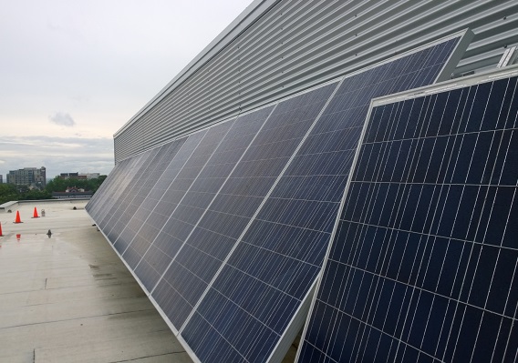
  • Developing technology that will power the world with low cost, environmentally friendly, and highly efficient concentrated solar cells
  • Greater global access through enabling broadband information access (internet, telephony, cable)
  • Working in areas allowing for communicating sound, vision and touch over optical networks 

Listed below is a mere sampling of research projects conducted at the uOttawa NanoFab:

Xiaoyi Bao - Nano-fibers devices for ultrasensitive sensing, quantum keys and low noise lasers

  • ​​​​​​Fabrication of nanofiber devices
  • Nanofiber devices and applications
  • Sensor networks
Top left - image of a bridge; top right - image of a pipeline winding through a forest; bottom left - image of a water dam; bottom right - image of a rocket ship on a platform

Structural health monitoring (SHM)

A schematic description of a nano-particle fluorescent light

Micro and nano-particle fluorescent light detection

Pierre Berini - Surface Plasmon Photonics

  • ​​​​​​Waveguides and passive elements
  • Telecom devices
  • Amplification
  • Lasers
  • Biosensors
  • Nanoantennas
  • Micro/nanofabrication
  • Integrated circuits
A schematic representation of an integrated circuit and biosensor set up

Integrated Circuits and Biosensors

A circle with colourful eyes and a tiger with CANADA written underneath next to a smaller circle with two colourful butterflies

Metasurfaces

Image of optical nanoantennas

Optical Nanoantennas

Ravi Bhardwaj - Nanoscale Manipulation of Material Properties in Solids with Light

  • Controlling interfacial properties
  • Plastic electronics
  • Direct laser lithography
  • Optical data storage in plastics
  • Embedded photonic devices
  • Laser processing of nanocomposites
  • Structured light-solid interaction
An image of a cantilever and microfluidic channel

Cantilever and microfluidic channels

Images of patterned cell growth

Patterned cell growth on PDMS

Image of a perfectly round ring next to thinner ring with a dot in the centre

Single pulse ablation of Si with Gaussian and OAM beams

Robert Boyd - Optical metamaterials

Two charts depicting the third-order nonlinear response through high and low intensity (n and α)

Origin of the third-order nonlinear response

Two schematic descriptions of photonic metasurfaces

A photonic metasurface

Paul Corkum - Attosecond photonics

  • Nonlinear light-matter interactions
  • Attosecond pulse characterization
  • Soft X-ray technology
  • Attosecond physics
  • Molecular imaging and dynamics
  • Imaging mass spectrometry
Multi-coloured spirals

A snapshot of an attosecond pulse

Image of an oscilloscope trace of the electric field

An “oscilloscope” trace of the electric field of a few cycle

An array of multi-coloured dots

A low energy electron hologram of N2

Karin Hinzer

Optoelectronic Devices

  • Ultra-high efficiencies: multi-junction solar cells
  • New concepts: materials, nanostructures, architectures
  • Photonic power: power-over-fiber, opto-couplers
  • Other devices: lasers, photodetectors, modulators

Systems

  • Concentrator systems: optical design, analysis
  • Outdoor testing: performance monitoring
  • Annual energy yield: concentrator PV, bifacial PV
  • Telecom: fiber, free space

Smart Grids

  • Smart grid intelligent control systems
  • Battery integration and load management
  • Smart sensors for Internet of Things

Solar Resource

  • Comparison of satellite to ground measurements
  • Model irradiance from limited data (ex. GHI→DNI)
  • Model spectrum from irradiance meas. (SolarSIM)
  • Nowcasting
Image of eight solar cells on a lawn next to a building with lots of windows

Outdoor testing - Lees Test Site

Professor Hinzer and a graduate student in gowns and hair nets looking at a sample in a petri dish in the clean room

Optoelectronic Devices

Two large solar cells on the roof of a building

Solar Resource

Benoît Lessard - Organic electronics: synthesis to prototype

  • Organic thin film transistors
  • Organic photovoltaics
  • Biosensors
  • Thin film/surface nano/micro engineering
  • Solid electrolytes/polymer dielectrics
  • Ultra pure semiconductive carbon nanotubes
Tweezers holding a thin transparent piece of material

Organic thin film transistor

An image of ultra pure nanotubes

Ultra pure nanotubes

An image of a biosensor

Biosensors

Jean-Michel Ménard - Ultrafast terahertz spectroscopy

  • Photonic crystal fibers
  • Time-resolved spectroscopy
  • Ultrafast phenomena
  • Semiconductors
  • Strongly correlated materials
  • Dynamical Bose-Einstein condensates (BEC)
A schematic representation of the noncollinear dual grating configuration

Noncollinear dual grating configuration

Raphael St-Gelais - Micro and nano systems

Microsystems at the interface of mechanics, photonics, and heat transfer, for:

  • Energy conversion
  • Acceleration sensing
  • Photodetection
  • Mid-IR light sources
Image of MEMS

High temperature MEMS for radiative thermal transport

Left is an image of two petri dishes filled with small SiN membranes, right is an image of a close-up of a SiN membrane held by a chopper blade

Silicon nitride high Q-factor nanomechancial resonators

Image of a mass-loaded SiN resonator

Mass-loaded SiN resonators for accelerometry

Arnaud Weck - Fracture and Femtosecond Research Ottawa Group (FROG)

  • Ultrafast laser-matter interactions
  • Micromachining
  • Surface texturing for: colours, wettability, catalysis
  • Creation of defects for material fracture studies
A schematic representation of CO2 reduction through sun and other catalysts resulting in CO, CH4 and C2H4 molecules

Catalysts for CO2 reduction

A circle with colourful eyes and a tiger with CANADA written underneath

Coloured silver coin obtained by laser irradiation

Lines of small dots in 5 rows

X-ray tomography of laser-induced microvoids in titanium